|
Recently I’ve been working with the Agilent U2001A power sensor. The U2001A is an averaging power sensor which simply means when the instrument is queried, that result is an average of multiple samples. If you want to easily measure peak power, you have to purchase the U2020 series power sensor, which costs more. However, the U2000A averaging sensor can be configured to create what is called a trace graph display, which effectively queries all of the individual points that go into the averaging the sensor is performing. Finally, software can be used to find the peak power measurement or simply display the measurement like a digitized waveform. To determine how to create the trace graph display I used the U2001A programming guide and the U2000 Series Labview driver from NI. The Agilent programming guide provides the example code, shown in Figure 1, to create a trace graph display. 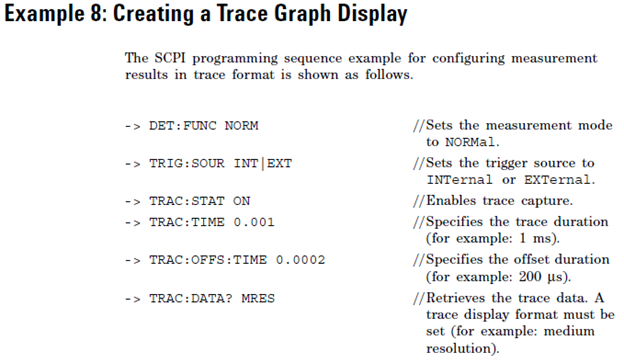 Figure 1. Example code for creating a trace graph display from the Agilent programming guide. This code is basically correct, but I feel like they left out a couple things. First of all I found that the trigger requires a little more explanation. The best way I found to do it was to trigger on a power level, their example doesn’t have this code. If you do not specify a trigger level it will just trigger immediate, but this doesn’t give as much control in some situations. Another thing I struggled with was how to decode the data returned by the instrument. The data is returned from the instrument in something called the IEEE 488.2 arbitrary block program data format. It took me a little while to find it, but the LabVIEW driver includes a VI to decode this data. I’m just pointing this out because the example from the programming guide doesn’t go into these details. Figures 2 and 3 show the LabVIEW code. The actual code is also available. 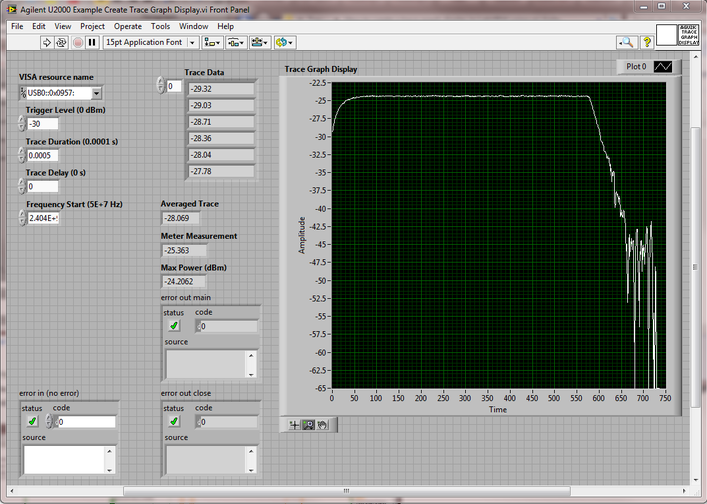 Figure 2. Front Panel of Example Create Trace Graph Display VI. A couple of things to note in Figure 2, the trigger level was set to -30 dBm. You can see from the graph that the acquisition begins at -30 on the rising edge of a pulse, there is a flat portion, and falls back into the noise. Also note the VI outputs: “Averaged Trace” is the average of everything on the graph, “Meter Measurement” is the average returned by the meter (I’m not totally sure why that doesn’t match the average computed in the software – I think the points acquired and the measurement points must not match) and “Max Power (dBm)” is the peak value found in the graph array data. 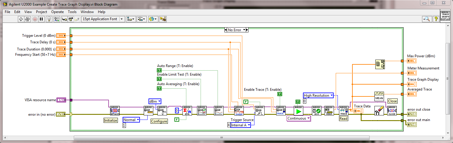 Figure 3. Block Diagram of Example Create Trace Graph Display VI. Figure 3 shows the block diagram of the example LabVIEW code. This code has quite a bit more configuration than the example code from the programming guide in Figure 1. Figure 1 shows the critical command and many of the extra commands I have in the LabVIEW code can be stripped out as they are just resetting the default values – I just felt this was more complete. As I mentioned earlier, one nice thing in this code is the U2000 driver implements the code to read the trace data. This capability is in the VIs “Read Trace.vi” and “Parse Data.vi” which are shown in Figures 4 and 5. You can also see that the driver has a comment with some details about the IEEE 488.2 data format. 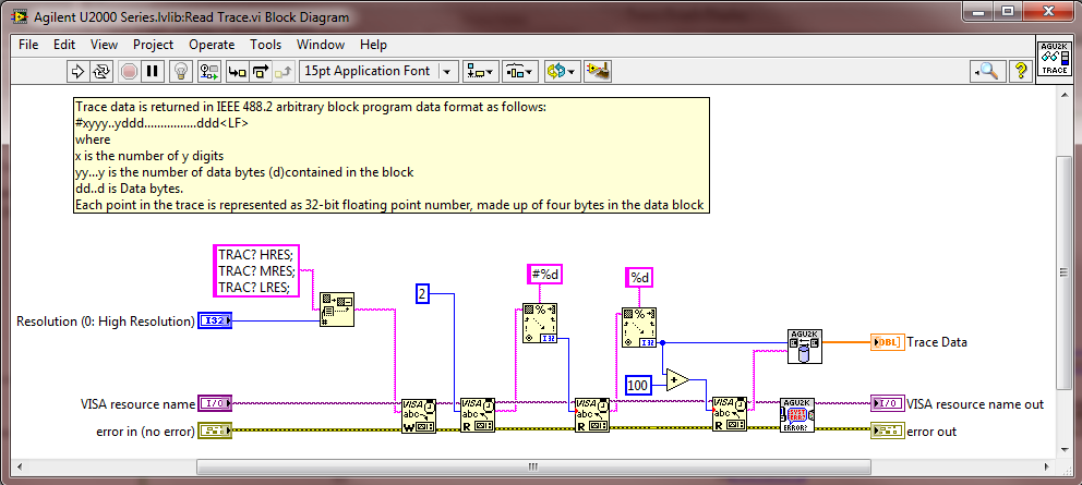 Figure 4. Read Trace.vi. 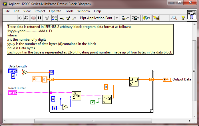 Figure 5. Parse Data.vi. One strange thing I found with this code is it seemed to work great if I kept the sub-VI “Wait for Acquisition Complete.vi” open, but if it was closed it seemed like code would hang-up a lot. Not sure what that is all about.
I posted this example code and you can download on this page, it is LabVIEW 2012. Note that I’m not providing the U2000 driver, get that from NI at the link above. Summary This post shows how to implement an Agilent U2001A power sensor trace graph display in LabVIEW. I feel this code provides a slightly more complete solution than the example code provided in the Agilent Programming Guide. Another useful feature of this code is it makes it possible to find the peak power of a measurement using the average power model power sensor.
0 Comments
I have previously written about how to do some basic things with the PXI instruments I have been working with lately. While I covered using the DAQ to generate and acquire analog signals, I would like to expand on what I wrote there. The NI PXIe 6259 M-series DAQ has three kinds of pins, or physical channels, as NI calls them. There are analog I/O, digital I/O and counter pins. The pins are setup like this. 32 analog inputs (ai0…ai31) 4 analog outputs (ao0…ao3) 64 digital pins (Port 0/line 0 to 31, Port 1/line 0 to 7, Port 2/line 0 to 7) where all of these pins are on Dev1. Dev1 is the DAQ, so if you added another DAQ to the PXI chassis it would be Dev2. Port 1 and 2 are arranged like this 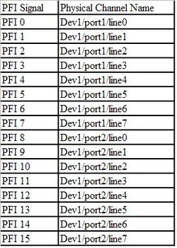 2 counters arranged like this 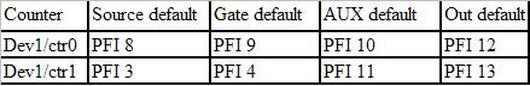 There is also PFI 14 which is FREQ OUT, used as a simple output only frequency generator. PFI stands for “Programmable Function Interface,” which is just a designator they gave it to mean it does something. There is some overlap between the digital pins and the counters. For example, PFI 4 is a dedicated digital pin used for ctr1 gate on counter 1. Digital I/O Example code written to demonstrate digital I/O of the DAQ is shown in Figure 1. The code uses the DAQmx driver to configure a digital input, output and clock signal. The output generates a sequence of digital values and reads them back in on the input when looped back through the matrix PXI card. Counter 0 is configured to be a clock signal where the frequency, duty cycle, initial delay and idle state of the clock are configurable. The digital input is setup to trigger off the clock signal and start acquiring data. The digital output is also setup to trigger off the clock and start generating the programmed data pattern. Notice that the digital output is set to update on the rising edge and the input on the falling edge. This will allow the output level to stabilize before it is read by the input. The clock, digital in and out are all configured to operate with a finite number of samples, 16 used here. It’s a little confusing, but in this case number of samples means clock pulses. Each of the clock, digital input and output are configured with their own task. The input and output tasks are started immediately after the channel is configured, in effect arming the channel as it does not really start until the trigger clock signal is received. Finally, the clock from the counter task is started. This starts the clock sequence and the code waits until the clock is finished allowing all of the digital data to be output and acquired. If I somewhat understand the NI terminology, a channel is created and controlled with a task. For example, you create a digital output channel and then any other code after that related to the channel has to be wired up to the use the same task where the task was created. You can also give the tasks meaningful names to help organize the code. It was a little confusing at first but become pretty intuitive quickly. I guess it’s like the instrument VISA session handles that some older NI drivers used, but you can use multiple tasks within the same instrument.  Figure 1. Digital pattern example block diagram Figure 2 shows the front panel of the code. 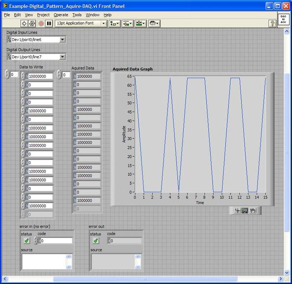 Figure 2. Digital pattern example front panel. In Figure 2 notice that the output and input are configured with only one line, where line 6 is the input and line 7 is the output. These are just arbitrary choices. What is significant is looking at the “Data to Write” array control, in order to set a value of 1 on the output line 7, I need to put a 1 in the 7th bit position (LSB on the right). “Data to Write” is formatted in binary to show this but really the driver accepts a U32 that covers the whole port. The same is true for a 0 value, Labview formats 00000000 as just 0 so it looks a little different than the 1. Also notice, the input line is line 6 so now the bit has moved a position in the “Acquired Data” indicator. You can also see on the graph that the Y axis is in decimal so a high value shows up as a 64. This would probably be a good place to create a new driver where if you are programming a single line only, you don’t have to keep track of the bit position. It’s pretty interesting because there are a lot of possibilities of how you can use this. With some pre-processing you could send a bit stream into a single line (basically, what is happening here) or you can program the whole port at once by just creating a channel as Dev1/port0 rather than Dev1/port0/line7. As also shown, you can split up the port so some of it is configured as input and some as output. Counter The digital I/O example made use of the counter as a clock to synchronize and trigger. The counter can also perform the operations typically associated with a counter, like measuring frequency, period and counting edges. Figure 3 shows the block diagram of an example using the counter to measure frequency. 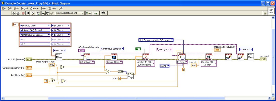 Figure 3 Block diagram measure frequency using DAQ counter The code is very simple. An analog output is connected to a counter input through the matrix. The analog output is configured to generate a sine wave and the counter is configured to measure the frequency. Notice that the programmed sine wave frequency is used to create a max and min value, plus/minus 10, of the measured frequency. This is wired into the counter configuration for accuracy. Figure 4 shows the front panel of the same code. 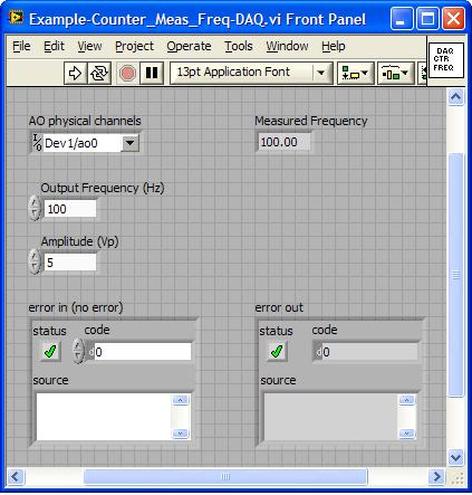 Figure 4. Measure frequency with DAQ counter front panel.
You can see in Figure 4 that the analog output frequency was programmed to 100 Hz and 100 Hz was measured with the counter. Summary This article showed some examples of using the NI PXIe 6259 M-Series DAQ. In addition to analog inputs and outputs the DAQ includes multiple digital I/O lines that could be used in a number of flexible ways. The counter is an additional useful instrument included with the DAQ. The DAQ is marketed as the all-purpose instrument and that’s what makes it interesting to work with. A DAQ can replace a number of more specialized PXI instruments like DMMs and function generators or it could be used to implement very specific high level cards like boundary scan controllers. Recently I’ve been developing a PXIe 1065 chassis based test system using Labview. The chassis includes an 8150 controller, a matrix card, a DMM, a DAQ and some power supplies. It’s a fairly simple set of instruments, but capable of many types of measurements. National Instruments supplies drivers to operate these cards but they require some effort to learn how to put them all together and create working test applications. I’d like to show some examples of how to make some basic measurements and some methods I feel are useful to improve on the supplied drivers. Note that this isn’t the real code I’m writing for my employer since I don’t want to give away any secrets or anything, but it is real working code. Initialization Before any of the instruments can be used to make measurements they all have to have instrument handles established. A good way to do this is by having a test application run an initialize routine that will create instrument handles for all of the instruments and hold them in a global variable. Figure 1 shows the block diagram to initialize the instrument handles for the Matrix, DMM and Power Supply and stores them in a global to be utilized by the application code later. The DAQ is not included, as it doesn’t require a handle to be initialized. The DAQ driver is a little different than the others; I’ll address this later. Figure 2 shows the global variable used to store these handles. 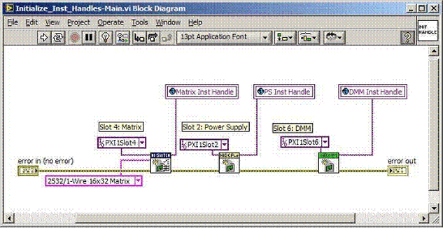 Figure 1. Initialize instrument handles for PXI instruments. 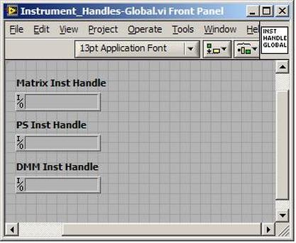 Figure 2. Global variable holding instrument handles (shown un-initalized) Matrix The matrix card is used for switching the instruments to the DUT. I’ve been working with a PXI-2532 16 by 32 crosspoint matrix. Additional hardware has been added as an ITA to make hard connections from the matrix inputs to the other instruments in the chassis as well as the DUT. That is, before you can use the matrix you have to wire the other instruments to the matrix inputs and wire the outputs to your test fixture and ultimately, DUT. Here is where the instruments are connected to the inputs of my system (omitting a couple I’m not discussing) 0. NA 1. NA 2. DMM V+ 3. DMM – 4. DAQ Counter Source 5. NA 6. NA 7. DAQ Analog Out Ch 2 8. DAQ Analog Out Ch 1 9. DAQ Analog Out Ch 0 10. Power Supply Out 2 +20V 11. Power Supply Out 1 +6V 12. Power Supply and DAQ Ground 13. Power Supply Out 3 -20V 14. DAQ Analog In Ch 0 15. DAQ Analog In Ch 8 The two essential Matrix drivers supplied by NI are Connect and Disconnect VIs, as shown in Figure 3. 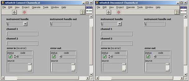 Figure 3. Connect and Disconnect driver front panels. Both VIs simply take the channel 1 input as the matrix input and the channel 2 input as the matrix output you want to connect or disconnect. For the 2532 matrix the input channels are R0…R15 and the output channels are C0…C31. Figure 4 shows and example of connecting the DMM at inputs 2 and 3 to outputs 1 and 2. Let’s say there is a 1k resistor at outputs 1 and 2. 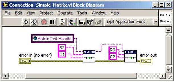 Figure 4. A simple matrix connection The code in Figure 4 will work but it’s not very flexible and it is pretty cryptic as to what is being connected. Some comments could be added to the code to say that the DMM is connected to a 1k resistor. But, a better way would be to create a new driver and give all the inputs and outputs meaningful names using some enumerated types. With a little more work a much more flexible Matrix control can be developed. Then new driver is called, Settings_Advanced-Matrix.vi. Unlike the simple code in Figure 4, it contains three modes: Set List, Clear List and Clear All. It also provides the ability to set multiple input to output pairs at once by accepting an array as input. The input and output designations have been given unique names as controlled by some strict type def controls. The advantage of the strict type defs is that the matrix input and output designations can be updated in one place and all instances of the control elsewhere will update as well. Finally, the code allows for relay debounce by calling the NI driver, “niSwitch Wait For Debounce.vi.” Figure 5, 6 and 7 show the block diagram of Settings_Advanced-Matrix.vi in the three modes. 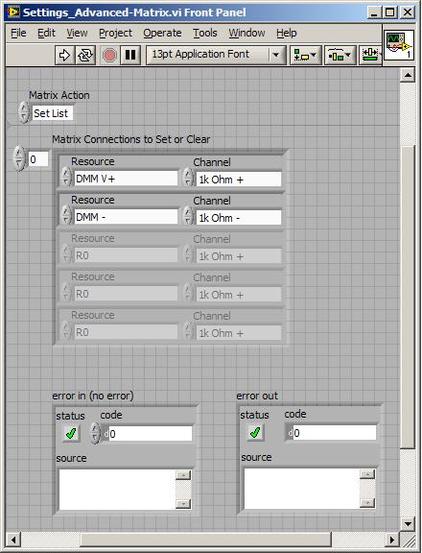 Figure 5. Front panel of Settings_Advanced-Matrix.vi 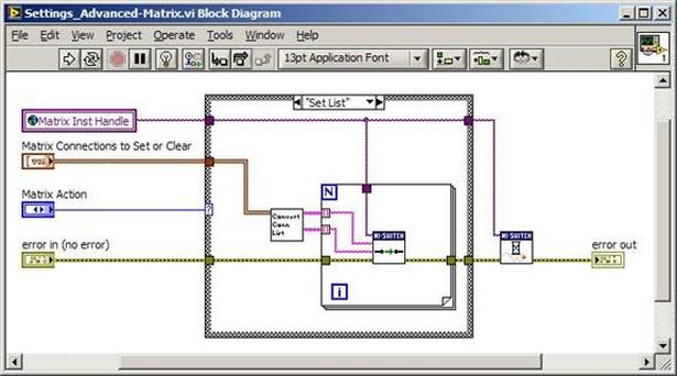 Figure 6. “Set List” mode of Settings_Advanced-Matrix.vi 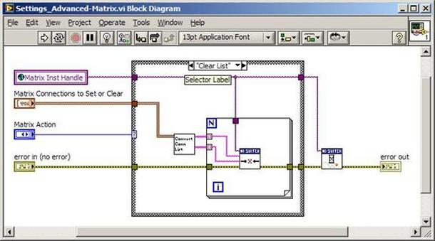 Figure 7. “Clear List” mode of Settings_Advanced-Matrix.vi 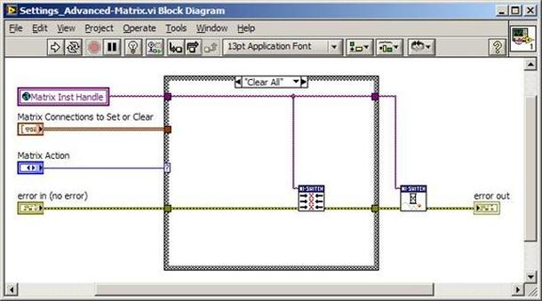 Figure 8. “Clear All” mode of Settings_Advanced-Matrix.vi In Figure 5 you can see the “Matrix Action” enumerated type control that allows the selection of “Set List”, “Clear List” or “Clear All.” It also shows that the VI has the ability to set multiple input to output connections at once and that the inputs and outputs have been assigned meaningful names. Figure 9 and 10 show the strict type defs used for the input and output names. Figure 6 and 7 show the use of a subVI called Convert_Connection_List-Matrix.vi. This VI is shown in Figure 11. 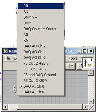 Figure 9. Resource (inputs) control strict type def 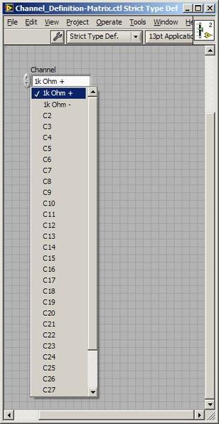 Figure 10. Channel (outputs) control strict type def 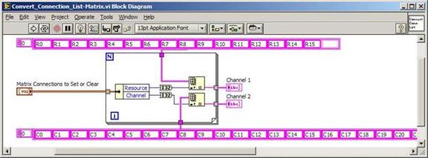 Figure 11. Convert Connection List block diagram Figure 11 shows how the array of meaningful resource and channel names are processed and replaced with the R0… C0… names that the NI driver uses. An additional enhancement that might be considered is if a certain combination of connections could cause damage to the instruments, error checking to prevent those combinations could be added. DMM Now that there is some code in place for making matrix connections we start using some of the other instruments present in the system. The DMM in the system is an NI PXI-4071. For the case of the DMM the drivers supplied from NI are pretty good, they could be wrapped but for my purposes here they will do. Figure 12 shows the block diagram of how to measure the 1k ohm resistor that is at outputs 1 and 2 of the Matrix. 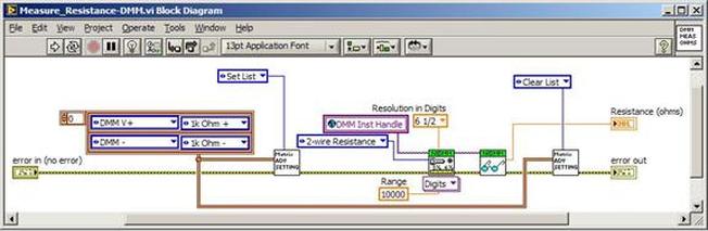 Figure 12. Measure resistance with a DMM through the Matrix. We can see in Figure 12 that the VI, Settings_Advanced-Matrix.vi developed in the last section is used to connect the DMM to the 1k ohm resistor through the matrix. The resistance is measured using the NI drivers niDMM Configure and niDMM Read. Finally, the matrix settings are cleared upon exiting the VI. A good way to ensure you have cleared the same relays you set is to wire the same constant to the set and clear matrix drivers. Figure 13 shows the front panel of the resistance measurement, showing that the VI read 1k ohms (note this is a 5% resistor and that is why it’s off from 1k) 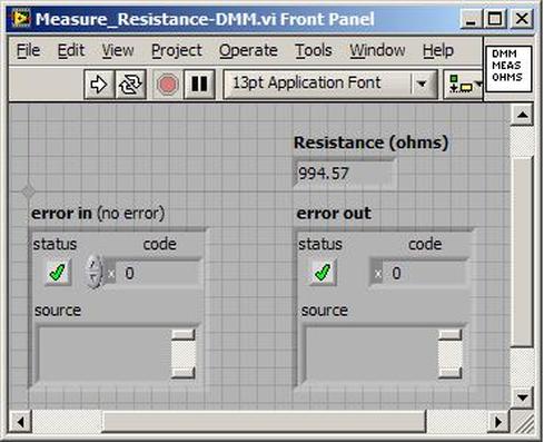 Figure 13. Measure Resistance Example. Now, let’s work in the power supply and use the DMM to measure voltage and current. Figure 14 shows an example of how to use the power supply to force current through the 1k ohm resistor and measure the resulting voltage across the resistor. 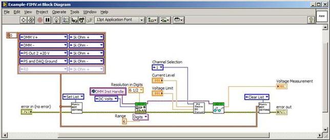 Figure 14. FIMV using the power supply and DMM. Following the code in Figure 14 we see that the matrix is setup to connect the power supply and the DMM to the 1k ohm resistor. The function, resolution and range of the DMM are configured followed by the power supply being set to source the current. Finally, the voltage measurement is taken with the DMM and the matrix settings are cleared before exiting. Figure 15 shows the front panel of the FIMV example. 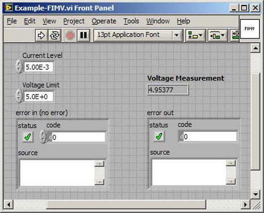 Figure 15. FIMV Example front panel. From Figure 15 we can see that when forcing 5mA through a 1k ohm resistor the result is roughly 5V. Figure 16 shows the code to force voltage and measure current. 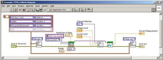 Figure 16 FVMI Example block diagram. In Figure 16 we can see that the matrix settings now apply the power supply to the 1k ohm resistor with the DMM connected in series with the positive power supply lead in order to measure current. The DMM is configured for range, function and resolution, the power supply is configured to force voltage and set the current limit, the current is measured by the DMM and the matrix settings are cleared. Figure 17 shows the front panel of the FVMI example. 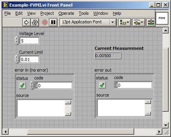 Figure 17. FVMI example front panel. From Figure 17 we see that when 5V is applied to the 1k ohm resistor with a current limit of 10mA, the result is 5mA. Figure 14 and 16 show that I didn’t really develop drivers for the DMM to configure them to measure DC voltage or current, I just use the NI supplied drivers. However, for the application of digitizing a waveform a driver is worthwhile to develop. Two VIs were developed to configure and perform a digitization, Figure 18 shows the block diagram of the digitize configure. 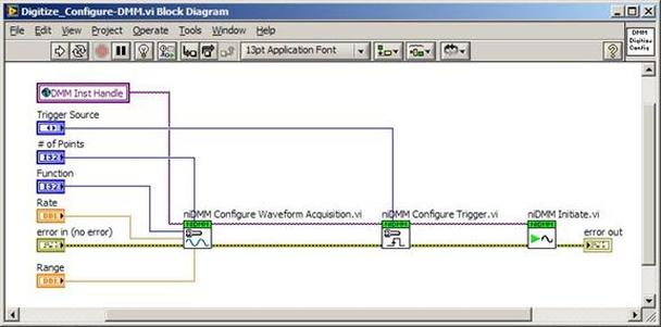 Figure 18. Digitize configure DMM driver. In Figure 18 we can see that there are three NI drivers used. The first is the configure waveform acquisition, this configures the DMM to digitize. Configure trigger, sets the trigger source to various trigger sources like, immediate or external. Finally, the initiate VI tells the DMM to arm and wait for the trigger. Figure 19 shows the front panel of the digitize configure DMM driver. 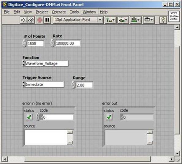 Figure 19. Digitize configure DMM driver. Figure 19 shows all the options that can be set for configuring the DMM to digitize. Most of the options are obvious, the rate is the number of sample per second. The range is the measurement range in the units that match the measurement function. Figure 20 shows the diagram of the digitize VI. 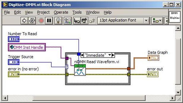 Figure 20. Digitize VI Block Diagram. Figure 20 shows the code that will send the instrument a trigger based on the trigger source and perform the digitization. Figure 21 shows the front panel of the digitize VI with a digitized sine wave being displayed. 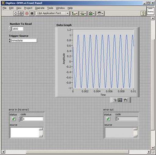 Figure 21. Digitize front panel. Figure 22 and 23 show an example of how to use the digitize drivers with some of the other code that has already been developed to digitize a sine wave. 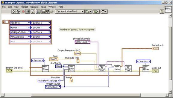 Figure 22. Digitize sine wave example block diagram. 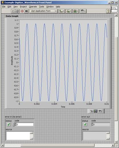 Figure 23. Digitize sine wave example VI front panel. Figure 22 shows the following operations to generate and digitize a sine wave. The first step is to connect the DMM and the DAQ analog output across the 1k ohm resistor. Next, the DMM is configured to digitize for 10ms and the DAQ starts to output a sine wave at 1kHz. Finally, the waveform is digitized, the sine wave output is stopped and the matrix settings are removed. We can see in Figure 23 that since a 1kHz sine wave has a period of 1ms and 10ms were digitized there are ten cycles digitized. Power Supplies While we used the power supply drivers in the FVMI and FIMV code in the DMM section to force the voltage and current we did not look at that code. The system contains the NI PXI-4110 power supply. Figure 24 shows block diagram for the Source DC voltage VI. 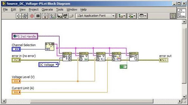 Figure 24 Force DC Voltage block diagram. Figure 24 shows all the NI drivers used to configure and output DC voltage with the power supply. First the power supply function is selected, followed by setting the voltage level and range (the range is automatically set to a predefined level based on the desired voltage level). The current limit is then set and the output enabled. Figure 25 shows the force DC current block diagram. 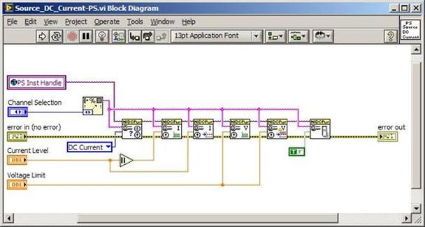 Figure 25. Force DC Current Block Diagram. Figure 25 shows a similar procedure as to set DC voltage. Set the function, set the level and range, set the voltage limit and enable the output. DAQ Again, in the DMM section the DAQ was used to generate a sine wave to digitize but this code was not examined. The system contains a 6259mx m series DAQ. Figure 26 and 27 show the DAQ drivers used to start and stop generating a sine wave. 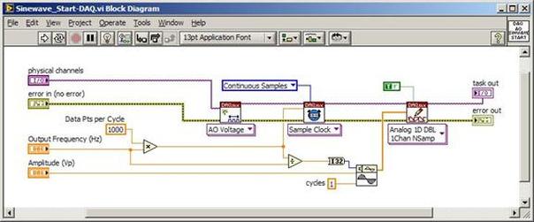 Figure 26. Sinewave Start DAQ VI. Figure 26 shows that it takes three steps to configure a DAQ analog output. First, a physical analog output channel must be selected and configured to output voltage. Next, the sample clock is configured to output data-points at the desired rate. Finally, a sine wave pattern is generated in software and programmed to the DAQ to be output at the previously programmed clock rate. This VI will begin outputting the waveform continuously as the sample clock was programmed to continuous samples. Figure 27 shows the sine wave stop VI. 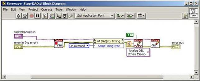 Figure 27. Sinewave Stop VI block diagram. The steps to stop the DAQ output shown in Figure 27 are to stop the task, write a zero to the analog output voltage and clear the task. Figure 28 shows the block diagram of an example of how to use the DAQ to digitize a waveform. 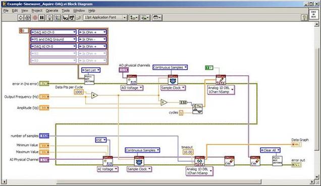 Figure 28. Example of waveform generation and digitization with the DAQ. In Figure 28 we can see that the matrix is used to connect a DAQ analog input to analog output through the 1k ohm resistor. The code to generate the sine wave is the same as from the DMM digitization example. The new code is used to digitize on the analog input and is very similar to the code used to generate the waveform. Replace the analog output channel with an analog input channel. Replace the write channel VI with the read channel VI. Finally, clear both tasks and remove the matrix settings. Figure 29 shows the front panel of the code in Figure 28. 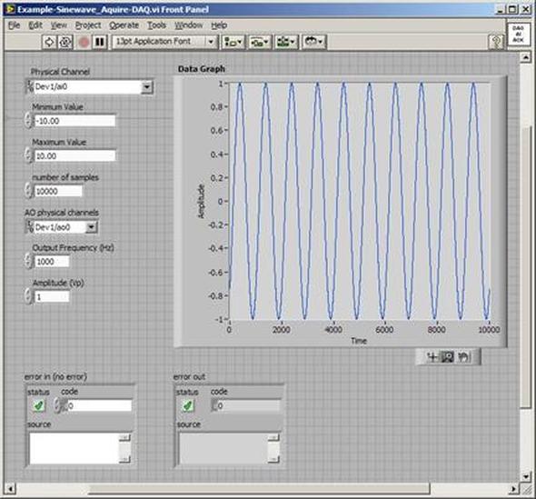 Figure 29. Front panel of digitize waveform with DAQ example
Summary PXI has become the standard for rapid development of flexible, low cost automated test systems. National Instruments with its Labview development environment is the industry heavyweight behind PXI based test. NI provides drivers for their PXI card instruments, however, these drivers can take time to learn and can often require additional work to make them robust instrument drivers. In this entry we saw some examples of how to build these drivers and how to use them to create some useful instrument functions. Some examples included, outputting voltages and currents, connecting instruments via a matrix card, generating waveforms and digitizing waveforms. I have previously written about digital boundary scan or IEEE Standard 1149.1. Analog boundary scan falls under IEEE Standard 1149.4 and is an extension of 1149.1 (it's actually called the mixed signal standard). While digital boundary scan is all about setting test bit values at inputs and output cells, analog is similar but adds test cells that interface with a test bus that can be used to route out internal analog signals to be measured. Analog boundary scan allows access to analog circuit nodes that may not be available through more traditional in-circuit test access. It allows parametric measurement of external components attached to IC or SOC pins along with the ability to hold or control the analog values going into the system at the pins. The trade off of is that the circuitry must be designed and implemented correctly at an increased cost. Figure 1 shows the basic parts that make up analog boundary scan when implemented. 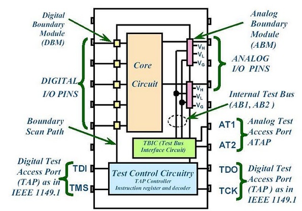 Figure 1. Analog boundary scan system. Referring to Figure 1 there are several components to notice. The system still contains digital boundary scan cells and the TAP controller. What is new is the TBIC (Test Bus Interface Circuit), the analog test access port (ATAP) with pins AT1 and AT2, the internal test bus (AB1 and AB2) and the Analog boundary modules (ABM). Analog Test Access Port (ATAP) The ATAP is made up of two pins, AT1 and AT2, which make up the external access to the analog boundary scan system on a chip. These pins are used to either read or apply analog signals into the chip. Test Bus Interface Circuit (TBIC) Figure 2 shows the internal switching of the TBIC.  Figure 2. Internal switching of the TBIC The TBIC is the switching (S5, S6, S7, S8) connection between the external analog boundary scan pins (AT1, AT2) and the internal test buses (AB1, AB2). The switches S9 and S10 allow the option to clamp the test buses AB1 and AB2 to a set voltage. These switches along with Vclamp can be used as noise suppression when the test buses are not in use. Also available is the ability to set the buses to either a high or low voltage via VH and VL. A threshold can be monitored on the test buses by comparing them to Vth. Internal Test Bus (AB1, AB2) The internal test bus is the connection between the TBIC and the analog boundary modules. It provides a method to read or write analog signals from the ATAP through the TBIC and on to the ABMs. Analog Boundary Modules (ABM) Like digital boundary scan modules, these modules are serial with the input and output pins of the IC. Figure 3 shows the details of the input portion of an ABM.  Figure 3. Analog Boundary Module Input Pin From Figure 3 we can again see the path from the analog tap AT1 through the TBIC and switching to the core of the IC. A switch SD is provided to isolate the core logic from the from the external analog function pin. This is useful to isolate the IC core circuitry from the external components that may be connected to either input or output pins. VH, VL and VG are also available to place a pin at high, low or constant voltage reference. Vth is available as a comparator for digital signals on the analog pin, so a pin can be monitored to be above or below a reference voltage. Example Application I have used analog boundary scan in my testing to test the leakage of capacitors connected to a pin. In Figure 3, if there were a capacitor connected to the analog function pin and I wanted to measure the leakage current, this is how to do it. The first step would be to put the system into EXTEST so that the core is isolated from the pin. Next, a power supply would be set up to apply a constant voltage through a DMM set to measure current and applied to AT1 or AT2. Finally, the cap is allowed to settle and the leakage current is measured from the DMM. Figure 4 shows how this is setup.  Figure 4. Setup for measuring capacitor leakage with analog boundary scan.
Summary Analog boundary scan falls under IEEE standard 1149.4 which is an extension of the digital boundary scan standard IEEE 1149.1. Analog boundary scan is extremely useful for making analog measurements when test access is limited or inaccessible. There are four main part of the system, the TBIC (Test Bus Interface Circuit), the analog test access port (ATAP) with pins AT1 and AT2, the internal test bus (AB1 and AB2) and the Analog boundary modules (ABM). The increase flexibility and test access is traded off with the increased costs to implement the system. Boundary Scan testing was created as a replacement for in-circuit testing in the 1980’s. The motivation was a number of trends that were taking shape with board technology that would limit testability. Some of the obstacles for in-circuit test were multi-layer boards. With a multi-layer it may be more difficult or impossible to probe internal layers with pogo-pins of an in-circuit tester. Other probing problems were evident with the advent of surface mount components and multi-side boards. Surface mount was shrinking boards to the point that there was no room to probe. Multi-sided boards complicate fixture design significantly, increasing test costs. A traditional in-circuit board test will look for the following defects. - Missing components - Damaged components - Opens and Shorts - Misaligned components - Wrong components Boundary scan took all of these defects into consideration and is able to test for them. Boundary scan is not an end all, it’s best to think of it as a tool in an effective test strategy. It’s not that good at doing functional testing or testing of ICs on boards themselves. Boundary Scan Technology Basics IEEE 1149.1 is the standard that defines digital boundary scan. There are a number of other follow-on standards that build in this one. The basic concepts of 1149.1 apply to all of the other standards as well. Boundary scan is something that has to be added to a new IC design while it is being designed and the designer can choose to implement the boundary circuitry any way they want but it should (but doesn’t always) follow the standard. Leaving out a lot of details for the moment, what happens is a boundary scan memory cell is put in-between an IC’s logic and its pins to the outside. Figure 1. shows this idea. This memory cell can then be programmed to either a 0 or 1 to artificially control the inputs and outputs to the IC. There is also a method to read the state of all the boundary scan memory cells. Using multiple boundary scan enabled ICs together, with the abaility to use these memory cells makes it possible to test for the in-circuit tests listed previously.  Figure 1. Boundary Scan memory cell between IC logic and external pin. Let’s take a more complete view of how this makes useful tests. 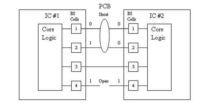 Figure 2. Shorts and Opens testing with boundary scan. Figure 2 shows how we can use boundary scan for testing for shorts and opens (the boundary scan cells are numbered for reference). The pins of the two ICs are connected together on the PCB. Keep in mind that these pins are routed to some other place on the PCB for a functional reason, the way the pins of IC 1 and 2 are connected is through the boundary scan cells, and these connections are just for testing. The whole boundary scan system is turned off when the board is actually being used and they have no affect. The short shown in Figure 2 is at the surface mount of the two pins on IC 1. Since we can read and write the contents of the boundary scan cells, we can set BS cell 1 on IC 1 to a 0 and BS cell on IC 1 to a 1 and read at IC 2 that both cells 1 and 2 read a 0. Similarly, since there is an open between the two 4 pins, the receiving pin will always show a 0. Boundary Scan Architecture There are four main parts to the boundary scan architecture. - Bypass Register - Instruction Register - Boundary Scan Register - Test Access Port (TAP) and TAP Controller The rest of these figures are from a really good boundary scan tutorial from Asset company (www.asset-intertech.com). There are four required pins that have to be added to an IC to operate the boundary scan system. - Test Data In (TDI) - Test Data Out (TDO) - Test Mode Select (TMS) - Test Clock (TCK) Figure 3 shows an IC with the boundary scan pins added to the package. 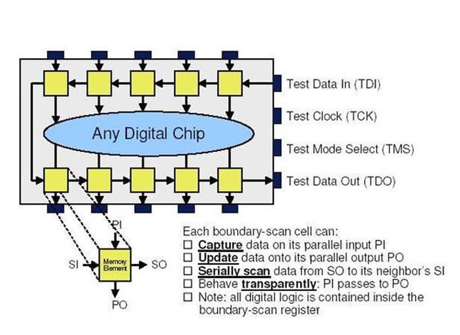 Figure 3. Boundary scan enabled IC. In Figure 3 you can see the parallel inputs and outputs along with the serial inputs and outputs. I talked about being able to read and write all of the individual boundary scan cells, this is accomplished with the serial input and output connections to each boundary scan memory cell. Data is written in and read out through TDI and TDO respectively in serial strings of zeros and ones. The TCK clock pin is used to clock this data in and out. TMS is a control signal used to coordinate all of these operations. Looking at Figure 4 we start to see how the four main pieces of boundary scan are setup. 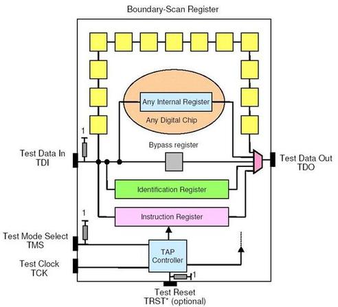 Figure 4. A boundary scan enabled IC showing boundary scan components In Figure 4 the yellow squares are the memory cells, these make up the boundary scan register. The Bypass register can be selected to put the IC into normal operation mode, bypassing the boundary scan system. The TAP controller is a state machine that interprets commands on the TMS input to control the boundary scan system. The instruction register controls the current operation of the boundary scan system and is programmed through the TDI input and controlled by the TAP controller. Although I didn’t mention it, Figure 4 shows an identification register. This can be used to store a unique identifier for that IC. Instruction Register The instruction register is where commands are loaded to the control the boundary scan system. Here are the steps to use the instruction register. 1. Using the TAP controller via the TMS input, the command is sent to connect the instruction register to TDI and TDO. This makes the register accessible to write commands to it. 2. A command in the form of a serial string is clocked into the instruction register using the TCK. 3. What are commands? The commands are putting the boundary scan system into useful configurations for testing. Here are some of the commands - Bypass – selects the bypass register between TDI and TDO - Sample – select the boundary scan register to TDI and TDO and sets the boundary scan cells to read the values being serially sent to them. - Preload – select the boundary scan register and sets the boundary scan cells to a known state. - Extest – select the boundary scan register and sets the boundary scan cells to a state where interconnect testing can be performed. Basically, isolates the IC logic for interconnect testing. - Intest - the boundary scan register and sets the boundary scan cells to apply their values to the internal IC logic. - Idcode – connects the identification register. - Clamp – This clamps the output pins to a constant state - Highz – puts the output pins in a highz state as in a tri-state output. 4. Upon sending the command to do so from the TAP controller, the command that was shifted into the instruction register is applied and takes effect on the system. Test Access Port and Controller When talking about the test access port that is really just the four inputs: TDI, TDO, TMS, TCK. The TAP Controller is where the TMS and TCK signal are interpreted. The TAP controller is implemented as a state machine that transitions states on the rising edge of TCK according to the value on TMS and updates the output from the TAP controller on the falling edge of TCK. Figure 5 shows the TAP controller state machine. 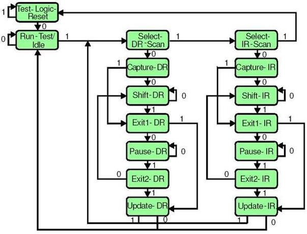 Figure 5. The TAP controller state machine. The arrows show the possible transitions and the numbers listed on the arrows are the TMS values that create that transition. There are states for the IR (instruction) register and the DR (boundary scan data) register. Going back to the procedure given in the instruction register section, sending a 0 – 1 – 1 would select the Instruction register. Then, holding TMS at 0 for the appropriate number of TCK high transitions would shift the command into the Instruction register. Finally, a 1 – 1 would update the Instruction register, update is what applies the command to the system. With the command sent, the states can continue on to the DR portion for shifting in test data strings. Boundary Scan Register The boundary scan cells located on the inputs and outputs pins are linked together in a serial string to form the boundary scan register. Figure 6 shows an example of how a boundary scan cell is designed. 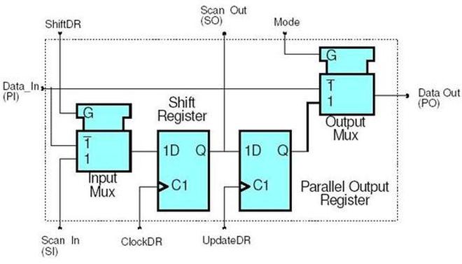 Figure 6. Boundary Scan Cell Design
Summary While there are endless topics that could be addressed related to boundary scan, I’ll leave it with the basics. The basic operation of boundary scan is - Scan in an instruction and apply it. - Scan in data and used it for testing. - Read back the data to find interconnect defects. The main pieces are - Instruction Register - Boundary Scan Data Register - Bypass Register - TAP and TAP Controller A test engineer has to make sure that the products they are assigned to test are operating correctly now and in the future. Before any products can actually be tested, a test system platform must be designed and built that can implement the engineers vision for an effective test. This entry will focus on building a test system from scratch. This entry will consider the high level issues as well as some of the low level design details. Strategy Building a test system is not the first task when a new product needs to be tested. Before you can start designing and building the system you must know what products are being tested and what measurements need to be made to test those products. In other word, first come up with a test strategy and then build your tester to implement that strategy. A test strategy is things like, what are the failure modes to check for and how much time and money should you spend on test. Before you can buy or build anything you also have to make some decisions about what type of strategy you have for your test system itself. That is, you need to decide on the architecture of your system. Here are some of the factors that go into deciding on tester architecture. What area of application is this test system going to be used? If you have a test strategy in place you will know this but it can affect the type of test system hardware you use to implement your system. 1. R&D testing If you are designing a test system for use while products are being developed, you need to make parametric measurements and have a flexible, informal setup that is fast to use. This may not be much more than an oscilloscope, but a more formal tester with some general software utilities may be called for. 2. Design validation and verification This is a little more formal than the R&D test system in that while it should be flexible for multiple different measurements, it may have to be able to formally record the results of the testing to create a record that the design worked as conceived. 3. Manufacturing test A manufacturing test system has to be fast and, hopefully, inexpensive. It has to be much more robust and automated. This is where most of the consideration of this entry will be. What is the scope of products for this system to test? Again, this will be most likely answered by your test strategy but you will need to know if it will be expected to test only as single product, multiple products or multiple product lines. What is the expected lifespan of this test system? Is it expected to be a general purpose test system that can test products which have not been designed yet? My though on this is it is better to try to make your systems simple and cheap, only testing a single or narrow line of products. I have personally seen several attempts to build universal, future proof systems/ITAs/fixtures only to have these projects grow out-of-control in time, budget and problems. Trying to build the ultimate end-all or universal system seems to be a trap that engineers often fall into. This may be a case of engineers trying to invent interesting but unnecessary projects for themselves. Some other factors to consider include expertise and hardware available, along with the development time and budget. If you have a lot of test developers with a lot of Labview experience, you may want to take advantage of that. Is there any existing hardware that your company already owns? Perhaps you have a number of older PXI systems with some hardware your people know well that is no longer going to be needed. Assuming this will not be an obsolescence problem that may be a time and cost savings to your project. Obviously, you have to build a test system that is appropriate to the budget you have available. Often, development time can trade off with cost. For example, you may be able to develop tests from more general-purpose instruments versus buying instruments (at a higher cost) designed for your exact test. Like an instrument that implements some special serial data protocol. The general architecture of a test system is usually based around a main bus. There are a number of bus options to choose from. A rule of thumb is that you should try to select a bus that has instruments available to perform 80% (if not all) of the measurements you need to make. Also, how well do the busses work together, like sending triggers and clocks across the bus types. An embedded controller for a PXI chassis will have GPIB and USB ports, but you should be sure the instruments can be integrated well. All of the test bus options trade off strengths and weaknesses including the following. 1. Bandwidth The bandwidth is a measure of the rate data can be sent across a bus in MB/s. So, as the bandwidth goes up the bus is able to transmit more data in a given period of time. This is an important consideration if you are trying to gather some kind or real-time high-speed data and will have to log it as fast as it’s acquired. 2. Latency Latency is the delay in the data transmission. This is different from the bandwidth where the bandwidth is more of the raw ability to transmit data; the latency is a more practical measure of how long it will take to transmit. Ethernet for example has pretty good bandwidth but poor latency. 3. Message based versus register based communication This is an instrument distinction you will often see that traces back to the bus the instrument is based on. Message based may be a little slower due to having to interpret the commands. Register based will directly write to the instruments registers, for fast binary data transfer. It used to be that register based instruments were much more difficult to program than message based instruments, but that is not really visible to the programmer anymore as the programming is all done with high-level drivers that mask the complexity. However, the drivers may slow down the performance gain of the register based. 4. Range of data transmission All the different bus types specify a maximum cable length for the instruments. LAN would be the best choice for long distances. 5. Instrument setup and software configuration It may be relevant that some instruments are plug and play while others require a system reboot. 6. Ruggedness of the system and connector How rugged is the connector for a particular bus? For example, USB is not a very rugged connector and can be easily un-plugged. There are several busses to choose from and I’ve probably missed several. Here are some popular ones 1. PXI/VXI/PCI (Card Cage) PCI card based instruments can be placed directly into a regular PC to put together a very simple test system. A PXI system and its newer variations are based on the PCI bus but go into a chassis to make a more rugged and dedicated test setup. The PXI chassis can then run off of an embedded or external computer and can work along side other standalone instruments. VXI is kind of old news at this point but they are pretty much the same kind of system as PXI. I have worked with both but I don’t think VXI was ever that popular. PXI, however, is an extremely popular choice and has heavy backing from National Instruments, so it’s fairly easy to get these systems going with Labview. 2. GPIB (Rack and Stack with standalone instruments) GPIB is usually used to connect stand-alone instruments. These types of instruments are different from card cage types in that they have a user interface on the front of the instrument for manual control or they can be programmatically controlled via the GPIB and PC. Because of the interface options, instruments like this may be a better choice if you want the option to do more manual, bench-top testing. They are also often mounted in test racks along with a computer to create an automated system. 3. Monolithic This is another option for test systems where you are not actually building the test system you just buy it and configure it to do what you need. Integrated circuit test systems often come like this. There are a lot of specific purpose testers, like manufacturing defect analyzers, flying probes testers, shorts and opens testers and in-circuit testers. Of course, you can perform all of these types of tests on systems you build yourself too. I have worked with test systems form Eagle Test Systems (now part of Teradyne) that are specifically for testing analog, mixed signal components and boards. While you still select the instruments you want they all come from the same manufacturer. They also develop their own programming environment. The advantage is you start with a nicely integrated test system, which is easier for some tasks (like automation with a handler) the disadvantage is it is more expensive. 4. LAN For remote monitoring applications Ethernet based instruments are available. A newer standard based on Ethernet is LXI. LXI adds triggering and synchronization to these instruments. 5. USB There is also instrumentation that can connect to a PC via USB that connect via plug and play. However, they are short range and do not a rugged connector. Test System Structure All test systems have a general structure with the following components 1. Instruments 2. System Control and Software 3. Switching 4. Rack 5. Power 6. Fixturing 7. Mass Interconnect/ITA Each area here merits some discussion and consideration. The remainder of this entry will cover the each of these areas. Instruments The instruments are the heart of a test system, and selecting your instruments is the most critical part of building the system. Selection of instruments is based off of knowing what measurements you are going to make. One approach may be as follows. Steps for selecting instruments. 1. List the input and output parameters you need to measure on your DUT. This could involve listing all the pins or test pads or whatever the access method is and then determining what needs to be done with them to get the measurements you need. So, do you need to measure voltage at a pin and report that? Do you measure the input and the output at two pins and use the values to calculate the gain? 2. List the accuracy and resolution needed for each measurement. Actually, you only need to look at the worst-case accuracies. For example, if you know that one of the measurements is really low current, you don’t really need to worry about all the other higher current measurements. As for resolution, this might show up if you need to accurately digitize some high-speed signal. In an application where you want to digitize some high-speed pulses for a certain length of time, a digitizer typically will trade off memory depth (number of samples) with acquisition speed. If you want to digitize really fast for a long time, that may take a more capable instrument. As a rule of thumb, the instrument accuracy should be at least 4x the desired accuracy of the measurement. 3. Check for redundant testing and instruments. Now you should be getting a better picture the instruments you will need in order to make all the measurements you need, but you still have not purchased anything yet. This is a good time to step back and see if you are duplicating any testing or duplicating any measurement capability. So, don’t just buy a DMM to do a measurement because that is what you would normally use to measure voltage. Maybe a DAQ that you are going to need for some other reason will have sufficient accuracy to measure that voltage, or maybe a power supply has the capability to measure voltage itself. 4. Will there be any need to do things in parallel? How many simultaneous DC signals will you need? This can affect the number of DAC channels you may need. How many waveforms will you need to apply simultaneously? If this is greater that maybe four, go with a card cage, otherwise a standalone rack instrument might be all you need. 5. Will you need any specialized instruments to implement specific test standards like a boundary scan controller? 6. Other instrument specs to consider – Noise, power, offset compensation, dynamic range, isolation. Some common instruments: 1. DMM – highest accuracy voltage and current measurements, slower speed 2. Arb, Digitizer, DAQ – Analog and digital I/O, able to generate patterns 3. Counter – sometimes part of a DAQ, counting and timing pulses, measure frequency. 4. SMU – Forcing and measuring analog voltages and currents. Goes beyond a DAQ for specialized applications like really low currents. System Control and Software In reality the first decision you may make in your head is what programming language you want this system to be. National Instruments Labview is the most popular choice at the moment. Some test engineers don’t like Labview but programming languages is one of those things that people really like to argue about. I feel Labview is the easiest to get a lot done fast, but it can also be easy to get yourself in trouble if you don’t know a few basic things about Labview. I plan to write another entry all about Labview in the near future. There are other choices like NI’s LabWindows/CVI and Microsoft Visual Studio .NET languages. NI clearly cares about and wants you to use Labview and these others are less common. If you are building a test system that will be used in a manufacturing environment you will need to have a user interface and a test executive. Well, you will need these things to have a serious test operation, I’ve seen places just getting started that didn’t have much of either. The test executive is what controls the test flow, handles sending your test results to a database and generates test reports. NI has a product that does all this for Labview called Teststand. NI also has templates for manufacturing test user interfaces that work with Teststand. Engineers love to come up with reasons why they should write their own test executive and user interface, but I would start with what NI provides and only go off on your own when you reach a serious road-block. Switching Switching can somewhat be seen as just another instrument but it really calls for a strategy all of its own. There are the following choices when it comes to switching. 1. No switching 2. Switching in the test system only 3. In the DUT interface hardware (ITA/Fixture) only 4. In both the test system and the interface hardware 1. No switching This is pretty rare, you almost always want the flexibility of some sort of switching but the switches add a little bit of resistance in the measurement path. For very sensitive measurements it may be required to connect the instruments directly to the DUT. This is also faster because you don’t need the software to operate the switches and wait for them to settle. The downsides are that it’s not flexible and not expandable. It can also be expensive because each instrument I/O point is completely dedicated to a signal DUT test point. 2. Switching in the test system only It’s easy to add switching to a test system by putting the switching in the test system itself. There are lots of PXI matrix cards and other types of switching modules available. This makes it easier to develop your tests because all the switching is controlled with software drivers that the manufacturer provides. If you leave open space in your card cage this is also an easy way to add more switching in the future. A downside can be that it can create some long signal paths. If you take the approach that all of the instrument outputs go out to a mass interconnect, to the DUT hardware, then back through the interconnect, through the matrix and back to the mass interconnect to finally arrive at the DUT, that can be a lot of wiring. This path is shown with the arrows in Figure 1. Some of the problem can be avoided by using parallel sense lines wired all the way to the DUT, but wiring length should be considered. Another problem can be that you are leaving long wires attached to your DUT that can act as an antenna for noise when that line is switched out. 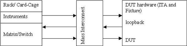 Figure 1. A long signal path through a mass interconnect and a matrix card. 3. In the DUT interface hardware (ITA/Fixture) only If all the switching goes in the DUT hardware, this should prevent a lot of the signal length problems described above because with the switches close to the DUT you don’t have to loop back to the system. This also solves the problem of have long wires on you DUT when switched out. The downside here is you need to design some sort of hardware to control your switches with software. There are relay driver components that can go on a PCB to provide the logical control of the relays, but you still have to figure out how to implement those. Another problem here is if all of your switching is going into a test fixture, in order to have any sort of reliability in your system, you’ll need to design a PCB. You have to have the tools and capability to design a PCB, designing a PCB is expensive and it’s not easy to change if there are mistakes or easy to expand in the future. 4. In both the test system and the interface hardware This is the most flexible option but also the most expensive. It’s flexible because, as was discussed, sensitive measurements are switched in the fixture and when accuracy is less of a concern the tester matrix can be used. There are a few different switching topologies available. 1. Simple Relays or FETs 2. Multiplexors 3. Matricies As with all things, try to keep the switching as simple as possible. Power and load relays are often separate from the instrument signal routing relays. Rack Designing and assembling the test rack is mostly just a list of things to remember to help ensure success. Even if you are just putting together a card-cage with a fixture, monitor, keyboard and mouse, these are things to consider. There isn’t much to the physical rack itself, you can buy them from many vendors and the instruments are a standard size to fit them. There are lots of rack mount PCs available also. Consider the following. 1. Assembly - Use the cables recommended by the instrument manufacturers - Secure all cables with strain relief - Make sure all cables are long enough - Use cable sleeves to keep things organized - Label the cables with what they are used for 2. Size - Leave some room to expand within the rack - How much floor space with the tester take and how much do you have - Leave space so everything fits, including the instruments and other hardware but also cables, power sources and PC. 3. Portability - Put wheels on the system - Make sure it fits through the door and it can be transported. Also, make sure it will fit in the space where it will be used. I have seen testers that were too tall to fit in the room where they were supposed to be used. 4. Safety - Interlocks – all the parts of the system should have interlocks where the tester will not operate unless a switch is closed that (ideally) is connected to a safety shield - Shields - EMO – Emergency shut-off switch somewhere easy to find. - Heavy stuff low – put heavy power supplies and UPS low in the rack so it will not tip over easily - Balance fixture shelf – if there will be a heavy fixture shelf where the DUT is connected, be sure this is not making the rack unstable. - High voltage points enclosed and disabled with interlocks 5. Environment of use - Ruggedized for its environment - What temperature and humidity is the room where the test system will be? - Altitude - Shock and vibration - Pollution level – will the tester be working in a dirty environment? 6. Ergonomics - Add some lights if necessary, particularly in the back side of the rack for looking inside - Work Space – What type of work surface will this tester need in a manufacturing environment? - Position for operators – will the operator stand or sit? Is the tester comfortable to use. How tall are the people using the tester? - Input devices – where do you put monitors, keyboards and mice? 7. Cooling - Add fans for air flow, maybe do some initial testing to see how hot the tester gets inside while running to see how many and how effective the fans are. - Instruments have their own individual fans, think about where these are blowing and if it is consistent with the overall cooling - Instruments often have specifications for ventilation that should be followed. 8. Signal Integrity and Grounding - Prevent long signal paths by designing DUT, switching and instruments as close together as possible. Add remote sensing lines for four-wire Kelvin measurements. - Terminate all grounds the same place, at the power distribution unit. 9. Maintenance - Setup a preventative maintenance cycle for cleaning fan filters and performing instrument calibrations - Replace worn parts - Provide some documentation or training for how to maintain the system Power There are two types of power to consider in a test system, system power and DUT power supplies. The systems power unit will provide AC power to the computer and all the instruments with some centralized controls. There might also be DC power supplies in the system specifically for powering fixtures and DUT hardware, it depends how you want to design it. The DUT power supplies are used to power your DUT itself (like 5V, +-15V rails, etc.), these are really very similar to the other instruments. Here are some power considerations 1. System Power - Does the system need power for different regions? 120VAC and 240VAC - Have an EMO button for emergency power off - Have a UPS in the system so if the power goes out it can be shut down properly - Consider the load that your system is. The total draw with all the instruments should be about 70% of the total available. - Determine a sequential power up method. If all the instruments are connected to one switch that inrush current could overload fuses or breakers. 2. DUT Power – power supplies have lots of specifications that may or may not be relevant to what you are doing. Here are some of them, I won’t try to explain it all here. - Settling time - Output noise - Fast programming of levels - Remote sensing - Built in voltage and current measurement – this is another alternative to adding expensive instruments - Physical size of the unit – power supplies can get big and heavy - Triggering options - Programmable output impedance - Output ranges, multiple outputs - Over load protections (V and I compliance) - Lead lengths - Safety Fixture I have already mentioned fixtures several times and I plan to write about designing fixtures as a separate article, but I’ll try to write some basic consideration here. The idea of a fixture is that you have to design some piece of hardware that will interface with the exact pin-out or test-points or whatever the method of your DUT. At one end are all the signal lines from the test system and the other end is the DUT interface. It makes the test system more reusable and also provides a place to put any necessary signal conditioning circuitry or switching. A fixture might also contain hardware to facilitate testing the DUT, like loads. Loads could be fixed value and location or programmable via switching. Some thought must also go into designing fixtures for operators to use in manufacturing. Are they rugged and ergonomic so that operators can easily place the DUT in them over and over without error or anything breaking? Are they easy to duplicate and deploy? ITA and Mass Interconnect The mass interconnect is a connector block where all of the instruments are wired out and made accessible. The mass interconnect consists of a receiver hardware piece attached to the test system that is populated with receiver modules that wire to the instruments. The ITA (interchangeable test adaptor) is the other side of the connector that interfaces the test system to the fixture. The ITA and fixture can sort of be a blurry line, which is which. The ITA may be just an interconnect, or it may contain switching and signal conditioning if it is desired to keep the fixtures very simple. The big advantage of the mass interconnect is it makes your test system reusable and general so different products can be quickly swapped and tested on the same tester. Figure 2 shows the block diagram of test system to DUT. 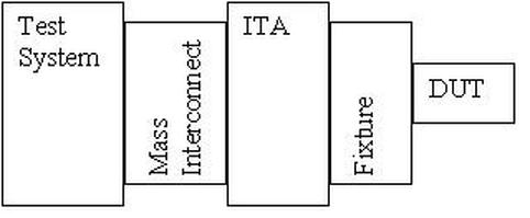 Figure 2. Test System to DUT connections
Summary Building a test system can be a pretty big job with a lot of factors to consider. Having a good test strategy and knowing what needs to be accomplished is key to building a successful test system. The main points are - Strategy – what kind of testing is being performed? R&D, Deisgn V&V or Manufacturing. What technology will the tester use? PXI-Card Cage or Rack based with standalone instruments. - Instruments – What instruments will you need to make the measurements you need to make? - System Control and Software – What programming language and support software will be used and is needed? What will be developed or purchased? - Switching – Where is the best place to put switching to meet the needs of your testing? - Rack – There are a number of items to remember to make a useful and useable rack. - Power – Two kinds of power, system and DUT. - Fixture – The fixture interfaces the test system with the DUT. - ITA and Mass Interconnect – The mass interconnect makes the test system generic so that multiple fixtures and DUTs can be tested. The ITA is used with the mass interconnect and works with the fixture. |
Archives
December 2022
Categories
All

|
 RSS Feed