|
I have previously written about digital boundary scan or IEEE Standard 1149.1. Analog boundary scan falls under IEEE Standard 1149.4 and is an extension of 1149.1 (it's actually called the mixed signal standard). While digital boundary scan is all about setting test bit values at inputs and output cells, analog is similar but adds test cells that interface with a test bus that can be used to route out internal analog signals to be measured. Analog boundary scan allows access to analog circuit nodes that may not be available through more traditional in-circuit test access. It allows parametric measurement of external components attached to IC or SOC pins along with the ability to hold or control the analog values going into the system at the pins. The trade off of is that the circuitry must be designed and implemented correctly at an increased cost. Figure 1 shows the basic parts that make up analog boundary scan when implemented. 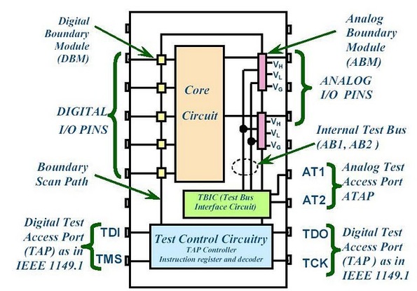 Figure 1. Analog boundary scan system. Referring to Figure 1 there are several components to notice. The system still contains digital boundary scan cells and the TAP controller. What is new is the TBIC (Test Bus Interface Circuit), the analog test access port (ATAP) with pins AT1 and AT2, the internal test bus (AB1 and AB2) and the Analog boundary modules (ABM). Analog Test Access Port (ATAP) The ATAP is made up of two pins, AT1 and AT2, which make up the external access to the analog boundary scan system on a chip. These pins are used to either read or apply analog signals into the chip. Test Bus Interface Circuit (TBIC) Figure 2 shows the internal switching of the TBIC. 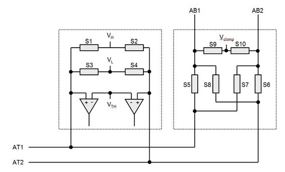 Figure 2. Internal switching of the TBIC The TBIC is the switching (S5, S6, S7, S8) connection between the external analog boundary scan pins (AT1, AT2) and the internal test buses (AB1, AB2). The switches S9 and S10 allow the option to clamp the test buses AB1 and AB2 to a set voltage. These switches along with Vclamp can be used as noise suppression when the test buses are not in use. Also available is the ability to set the buses to either a high or low voltage via VH and VL. A threshold can be monitored on the test buses by comparing them to Vth. Internal Test Bus (AB1, AB2) The internal test bus is the connection between the TBIC and the analog boundary modules. It provides a method to read or write analog signals from the ATAP through the TBIC and on to the ABMs. Analog Boundary Modules (ABM) Like digital boundary scan modules, these modules are serial with the input and output pins of the IC. Figure 3 shows the details of the input portion of an ABM. 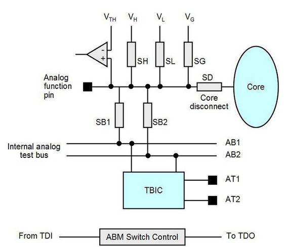 Figure 3. Analog Boundary Module Input Pin From Figure 3 we can again see the path from the analog tap AT1 through the TBIC and switching to the core of the IC. A switch SD is provided to isolate the core logic from the from the external analog function pin. This is useful to isolate the IC core circuitry from the external components that may be connected to either input or output pins. VH, VL and VG are also available to place a pin at high, low or constant voltage reference. Vth is available as a comparator for digital signals on the analog pin, so a pin can be monitored to be above or below a reference voltage. Example Application I have used analog boundary scan in my testing to test the leakage of capacitors connected to a pin. In Figure 3, if there were a capacitor connected to the analog function pin and I wanted to measure the leakage current, this is how to do it. The first step would be to put the system into EXTEST so that the core is isolated from the pin. Next, a power supply would be set up to apply a constant voltage through a DMM set to measure current and applied to AT1 or AT2. Finally, the cap is allowed to settle and the leakage current is measured from the DMM. Figure 4 shows how this is setup. 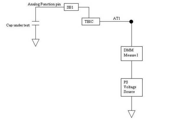 Figure 4. Setup for measuring capacitor leakage with analog boundary scan.
Summary Analog boundary scan falls under IEEE standard 1149.4 which is an extension of the digital boundary scan standard IEEE 1149.1. Analog boundary scan is extremely useful for making analog measurements when test access is limited or inaccessible. There are four main part of the system, the TBIC (Test Bus Interface Circuit), the analog test access port (ATAP) with pins AT1 and AT2, the internal test bus (AB1 and AB2) and the Analog boundary modules (ABM). The increase flexibility and test access is traded off with the increased costs to implement the system. |
Archives
December 2022
Categories
All

|
 RSS Feed