|
When testing a new chip design there is a lot of work that goes into characterizing the design to determine if it meets specifications. One such type of testing is characterizing an ADC. DC Evaluation, Gain and Offset The purpose of an ADC (Analog to Digital Converter) is to take a continuous time analog signal and convert it into a discrete time digital signal. We talk about ADCs in terms of bits. So you might have a 4 bit ADC which means that the full scale analog value that can be an input to the ADC is divided by 2^4. 
And (let’s say) 1.0 volts is your full scale input. Then, 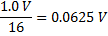
So, each digital step after the ADC conversion represents 0.0625 volts. Now this is an ideal behavior, in reality no ADC will work perfectly like this. The Gain of an ADC can be defined as follows: 
The offset of an ADC is defined as voltage difference between corresponding inputs and outputs. This may not be the same for all inputs, but an average of all the offsets at each, or several inputs would serve as a good general offset number. ADCs are statistical in nature One unavoidable problem with an ADC is it’s inherent statistical nature. If you think about how an ADC works, multiple analog voltages will result in the same digital voltage output. The extent this is seen is dependent on the resolution of the ADC. As shown above in the 4 bit ADC calculation, each digital step corresponds to a finite voltage value. If the input voltage to an ADC happens to fall right on the edge of transitioning from one level to the next then some of the time you will get the smaller code some of the time the larger code. That's what I mean by statistical, given enough data you can determine what percentage of the time the ADC will output what code. Ideal and Non-Ideal ADC In an ideal ADC each code would have a uniform width and center point. Figure 1 shows an ideal ADC curve of a 4 bit ADC. In reality, an ADC is non-ideal, which can be observed in the following ways: Codes are non-uniform Figure 2 shows an example of a code that is longer than the others. Code transitions are not clean Figure 3 shows and example of code transition that is not clean. That is when the ADC is tested as it approaches the code transition point the code might bounce back and forth a few times before transitioning. 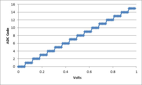
Figure 1. Ideal ADC Transfer Curve
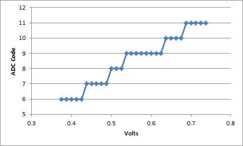
Figure 2. Code 8 and 9 are not uniform
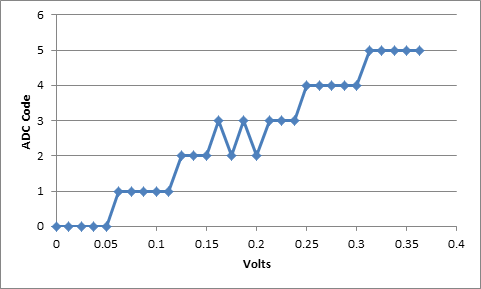
Figure 3. Example of an indefinite transition point from code 2 to 3
ADC Transfer Curve Figure 1 is an example of an ADC transfer curve, plotting input voltage vs. ADC code. Plotting the transfer curve is how to characterize the ADC. There are a lot of different methods to characterize the ADC and ways to generate the transfer curve. I'll describe the linear ramp method I have experience using. Linear Ramp ADC Characterization Here is the basic setup to characterize and ADC with a linear ramp. 1. Set a function generator to create a slow ramping voltage starting at the minimum voltage input and ramping to the maximum voltage input of the ADC. The ramp should be slow enough that multiple input analog voltages will result in the same output code. I'm talking at least 10 here. This will allow you to see the transition points clearly. 2. Setup the ADC to read codes for the entire time that the linear ramp input is on. 3. Save the ADC output somehow, this is probably read out of some memory in the system with a script like in LabVIEW or Python (some programming environment) 4. Plot the transfer curve. You may want to do a few trials or try a few instances of the ADC for repeatability and reproducibility study. Characterization Calculations Once you have gathered your ADC data, there are a few calculations to make that will gauge the performance. 1. Find the edges In the ideal ADC transfer curve it is obvious where the code edges (transition points) are, but in a real ADC it is not as obvious. What you have to do is create a histogram of the ADC output codes. All this does is group the like codes back together at the transition points and create a clean transition point. So, if you look at Figure 3, it is not clear where the transition from code 2 to 3 is. Creating a histogram basically moves all the output codes of 2 together on the left and moves all the output codes of 3 together on the right. This creates a clean transition edge. While we can’t really be sure this is the real edge of the ADC this is the best we can do to move forward with our analysis. 2. Generate the Ideal ADC Transfer Curve This is just a matter of creating an ideal curve like shown in Figure 1. 3. Calculate the Monotonicity Calculating the monotonicity is a measure to verify that each output code will be larger than the previous one when an increasing signal is being applied as input. This is probably not that likely to be a problem when the input signal is slowly increasing (or decreasing) ramp signal. Here is the equation for monotonicity: 
For a 16 bit ADC i is the steps 0 to 15 and S(i) is the voltage equivalent. And, S(i+1) is just the next higher point. 4. Calculate and plot the DNL – Differential Nonlinearity DNL is a measurement to determine how uniform the output code step sizes are for a linear ramp input signal. 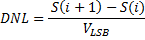
For the 16 bit ADC 
5. Calculate and plot the INL – Integral Nonlinearity INL is a measure the ideal ADC transfer curve versus the actual transfer curve. 
What is equation will do is when you plot this line it will exaggerate the places where this curve deviates from the ideal line and you will get a good snap-shot view of the linearity.
Summary The important aspects to characterizing an ADC are to determine the gain, offset, DNL and INL. The steps to characterizing an ADC are to: Determine your input voltage range, setup your experiment, gather the data and analyze the data.
2 Comments
|
Archives
December 2022
Categories
All

|
 RSS Feed