|
IQ Signals I’ve been recently reading a few journal articles about RF testing (see here) and since I don’t know much about RF or communication, I’ve been reading about some of the basics. Here is what I’ve learned about IQ signals. IQ signals or IQ data are used in RF modulation circuits. When modulating a signal you are basically taking a sine wave signal and altering the amplitude, frequency or phase in order to encode information. It turns out that building a circuit to control phase precisely is difficult, but controlling amplitude is easier. Using an IQ signal you can change the amplitude of two separate signals to control the phase, frequency and amplitude of another signal. The two signals are the I and Q (I for In-phase and Q for quadrature or 90 out of phase). A sine wave represented in a polar coordinate plane looks like this: 
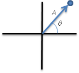
Figure 1. Sine wave represented with a polar coordinate system Converting from polar to rectangular coordinates the real and imaginary portions of the vector become the I and Q signals. Like this: 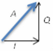
Figure 2. I and Q signals are the real and imaginary components of the rectangular coordinate system representation of a sine wave. So, I think it’s easy to see from Figure 2 that changing the amplitude of the I and Q signals can modify the amplitude, phase and frequency of the sine wave in the polar coordinate system. A typical IQ modulation circuit looks like this: 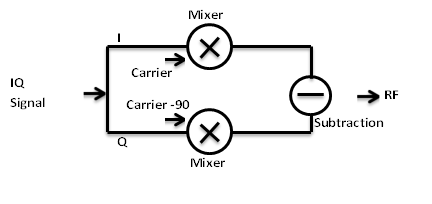
Figure 3. Circuit to implement IQ modulation
You can see in Figure 3 how the I and Q data signals are mixed with the carrier signal and subtracted to create the RF modulated signal. The subtraction is part of the mathematical conversion from rectangular to polar form. I pretty much learned all this from one place, a white paper that NI put out (here). They seem to have a number of good articles about basic RF information and RF measurement information. As usual, I’m a big fan of NI.
0 Comments
In my previous post I went over all the steps to fabricate a PCB. This post is all about taking the finished PCB bare board and assembling it with components.
PCB Assembly Process There are two main type of PCBs, namely, through-hole and surface-mount. The assembly process for any board is basically this: 1. Populate the board with components 2. Solder the components But there is some difference between through-hole and surface mount. Through-Hole Assembly Process In addition to the steps above there is also trimming the through-hole component leads and cleaning the flux. Through-Hole Soldering Flux is applied before solder to break down the oxide that may be on the pad and allow the solder to flow. Some solder includes flux in it. For hand soldering this is called flux core solder. Solder can be either hand soldering or some type of automated soldering. Wave soldering is the most common type of automated soldering for through-hole boards. What happens is the wave soldering machine contains a large reservoir of molten solder that is being agitated to create two waves. The first wave is a turbulent wave that helps to break the surface tension of the solder and get it into the holes. The second wave is a laminar or smooth wave that has a finishing effect. Another method to solder through-hole components is to spread solder paste into the holes, populate the components and then run it through a reflow oven. The disadvantage with this is the components are being heated where with wave soldering the whole component is not heated, just the leads. Cleaning Flux has to be cleaned off of the board after soldering. This is done with a solvent chemical or an aqueous (mostly composed of deionized water) method. Some flux is considered no-clean, it has the advantage of being faster and more environmentally friendly. However, it can affect the appearance of the board and interfere with test probe contact as well as adversely affecting rework efforts and lessening the adhesion of conformal coatings. Surface Mount Technology Assembly Process The basic surface mount process is as follows: 1. Apply solder paste to the component lands 2. Place the components via pick-and-place machine 3. Reflow the board to melt the solder and secure the components. 4. Underfill/Encapsulation/Finishing For a multilayer board, these steps are done on the bottom side and then the board is flipped over and the top side is done. The only difference is since the bottom side components are reflowed twice, the second time while upside down, there is a chance components could fall off. The components will only fall off if the weight of the component is such that it is greater than the surface tension of the solder holding it on. If this is the case, an adhesive is added to the component to hold it on during the second reflow cycle. Apply solder paste Solder paste is a mixture of tiny solder balls, flux and other chemicals. It is most often applied by stencil or screen printing. It can also be dispensed directly to the board. Some components are not well suited for solder paste. Direct chip attach, like flip chip technologies typically have area array connections that are too small to use solder paste. In this case, flux is applied to the circuit board pads and is used to hold the chip in place. Then, during reflow the solder balls on the chip provide the solder to hold it on the board. Another method to apply flux is to dip the chip solder balls into a bath of flux and then place it on the board. Place Components There are two types of common pick and place machines, turret or gantry. The turret type is where a board is on a conveyor and stops by a round turret that spins a picks up components off of another line and puts them on the board. This is more often used for passive components. The gantry machine is where the board is stationary while an X-Y type placement machine goes and gets the correct part from the feeder supply. This is used for larger components like ASICs. Reflow Reflow is done as either a batch or inline process. In an inline oven, the board will go in one side unsoldered and pass through increasingly hotter temperature zones before passing out the other with the soldering complete. The objective of the temperature profile is to get the board hot enough that all components are soldered but not so fast that they are damaged by the heat. Batch furnaces provide a vacuum condition where inline usually do not. The inline types are more often used for high volume production. Cleaning Cleaning considerations are similar to those of through-hole boards above. Finishing and Underfill For some very fragile components or boards that will be used in unusually harsh environments, it may be necessary to use some encapsulant material to cover all the components and protect them. Underfill is done after soldering and is the process of filling the void under chips, especially direct chip attach technologies like flip chip that need additional mechanical stability. Underfill is applied with a capillary action. Capillary action is where the underfill is dispensed next to a chip on a board and the surface tension of touching the chip pulls it under to fill the void. The most important aspect of encapsulant and underfill is to ensure there are no voids after it is applied. This can leave air and moisture inside that can cause all kinds of reliability problems and failures. Summary The methods of assembling a through-hole and surface mount circuit board were presented. The main tasks in assembling a board is populating components and soldering those components in place. There are other considerations like, cleaning and encapsulation. As I was saying in my previous post, I have started a new job and I want to write about some new topics. I have been working for some time now on learning more about PCBs, but there is a lot to learn.
When I wrote about Test Engineering, I felt like more of an expert. This post is more of a learning exercise, trying to get some background on the subject. Hopefully, someone else can get some use out of it too. This is a pretty basic overview, I didn’t try to learn much about all the chemistry that goes into it, but that’s a huge part of it. All that detail is omitted here. That being said, my two main sources of information are the books: Printed Circuits Handbook, edited by Clyde F. Coombs, Jr. and Complete PCB Design Using OrCAD Capture and PCB Editor by Kraig Mitzner. Traditional PCB Fabrication Process There are a number of process flows for making a PCB. These processes are for producing a muti-layer board. The process is a little different if you are going to have buried or blind vias. Process for a standard inner layer 1. Clean 2. Apply photoresist 3. Apply the photo-mask 4. Expose the photoresist pattern 5. Develop the photo resist 6. Etch the copper 7. Strip the photoresist Process for an inner layer with vias 1. Drill via and tooling holes 2. Plate the via holes with copper 3. Apply photoresist 4. Apply the photo-mask 5. Expose the photoresist 6. Develop the photoresist 7. Etch the copper 8. Strip the photoresist Additional steps to finish the board 1. Laminate the layers together with B stage laminate 2. Apply solder mask/resist 3. Apply the surface finish – to prevent copper oxide Hole drill and copper plating Via holes are drilled with either a mechanical drill bit, a laser of a masking chemical method. Copper is deposited by a method called electroless copper (chemical), electroplating or direct plating. Electroless copper is where the surface is cleaned and a catalyst is applied to the surface. The catalyst is there to attract the copper to the surface. The board is put into a chemical bath that includes copper and the copper is attracted and plated on the surface. This is just applying a seed layer, other methods are used to bring the copper up to the desired thickness. Direct plating is the broad term for a number of other chemical methods. These are newer methods that are more environmentally friendly than electorless copper. Electroplating is where the surface that is to be plated with copper is charged and an oppositely charged solution of copper is applied to creating the plating. You can only do this after either electroless copper or direct plating has been done to create a seed layer of copper to charge. Imaging Imaging is the process of applying the photoresist, masking and developing it. The purpose of photoresist is to create a mask to remove copper to create the circuit pattern. Photoresist is a photo-sensitive material that is applied on top of the copper. Photoresist can be a liquid or dry film type. A mask is placed on top of the photoresist and UV light is applied. The mask is a stencil pattern of the copper, exposing some of the copper, and shielding other of it from the light. Depending on the type of photoresist – positive or negative – either the copper you want to stay or the copper you want to remove is exposed. That is, in a positive photoresist the portion that is exposed to UV light breaks down and can be removed by a chemical bath. So, with positive resist, the mask would expose all the waste area and that is what would be removed leaving photoresist to cover your actual circuit pattern. In the case of a negative resist, the portion that is exposed to the UV light is hardened and will stay and the shielded portion of the resist is removed. This means that the stencil applied to the resist will expose the actual circuit trace. The circuit board is then put in a chemical bath and the part of the photoresist that was exposed (or not exposed) to the UV light will be removed to create the circuit trace pattern. This is called developing the photoresist. Laser Direct Imaging (LDI) There is also an alternate method to photo imaging where a laser is used to image the photoresist instead of using a mask. So, with positive resist - laser over all the waste area or outline the pattern With negative resist - laser the pattern itself and the non-lasered (non-exposed) will be remove by chemical bath. Etching Now that the copper layer has the circuit pattern in photo resist on it, the waste copper can be etched away in a chemical bath to leave only the circuit traces. Process type This process of imaging and etching is called a subtractive process because you start with a full sheet of copper and remove some of it to make traces. There is also such a thing referred to as an additive process, where you start with a blank substrate and add the copper traces by some method. Additive processes are newer and not used as much. Laminate Once you have all of your copper layers patterned, they are aligned and laminated together with layers of semi-cured epoxy-resin called B-stage. The patterned layer substrates are fully cured and called C-stage. The patterned layers are stacked with a B-stage between each one and pressed and cured. One other thing to know about this, copper does not stick to epoxy that well, so the copper surface must be treated before gluing. One way to apply an oxide treatment to the copper called brown or black oxide. Some copper is already treated by the supplier of the foil laminated sheets. Solder Mask Solder mask or solder resist is applied to the entire board with the exception of the areas where solder is to be applied, like on surface mount pads. Solder mask can be photo-imageable or not and it is applied by screen printing, spray or curtain coating. Screen printing is more difficult with very small circuit features. It is important that solder mask be removed from holes, especially plated through holes that are to be soldered. Solder mask is left on the finished board and helps provide protection to the board surface. Incidentally, solder mask is usually green and that is what gives circuit boards their green color. Surface Finish The point of the surface finish is to put a metal over the copper pads that will protect it from oxide until is it time to solder to it. Some common surface finishes are: 1.Hot air surface level (HASL) – dip the board in solder and pull it out, removing the excess solder with air-knives. This traditionally uses leaded solder, so it’s not that popular any more. 2. Eletroless Nickel Immersion Gold (ENIG) – here electroless nickel is applied to the pads and then it is dipped in Gold. Gold will not oxidize and will mix well allow soldering. 3. Organic Solderability Preservative (OSP) – this is a very thin organic coating that is applied to the copper. 4. Immersion Tin – prevents oxide but can lead to “wiskers” which form and lead to shorts that are difficult to test for. HDI HDI which stands for High Density Interconnect, is the name given to a group of techniques used in PCB fabrication and design. The main difference that defines HDI is the use of micro-vias versus traditional plated through holes (PTH). The difference being where a PTH goes all the way through a multi-layer board, the micro-vias are either buried or blind and do not go through all the layers. A buried micro-via is one that connects to internal layers of the board but does not extend to either side of the board. A blind micro-via is one that extends from one side to an internal layer but not all the way through. So, what makes this use of micro-vias high density? When building surface mount boards the micro-vias can connect different layers but there does not have to be space left for a PTH to go all the way through the board and pass through layers it is not connected to. This enables putting different surface mount components and their routing on both sides of a board, with more flexibility. The advantages of this may be obvious, but this is one factor that enables super high tech mobile devices to be so small and light. Advantages include: More, smaller components on a board, finer routing density (since you don’t have to make room for all those PTHs) and shorter signal paths. Flexible Circuit Boards A number of the products we use at my company are implemented on a flexible circuit, this is common in the medical device industry. Flexible circuit boards are used for two main reasons. 1. When circuits need to be flexible for the operation of the device - like a hinged laptop screen. 2. When space is at a premium. In this case a flexible circuit may not have to flex but it has to be extremely thin to fit in a small space. Related is the idea of flying leads, this is a portion of the flexible board that will be folded one time to fit into a small space or make a 3D type circuit board. Materials The dielectric substrate layers of flexible circuit boards are typically made out of polyimide or polyester. Polyimide is more expensive and more stable at high temperatures. For this reason it is used for soldering applications where polyester cannot be soldered. Copper is used for the conductors and the preferred type for flexibility is called rolled annealed (RA) versus more traditional electrodeposited (ED) copper. An adhesive like epoxy is used to stick the copper foil to the laminate layer, although there are adhesive-less laminates available as well. Finally, a coverlay material is used in replacement of solder mask as used on traditional rigid boards. In addition to the function of solder mask, the coverlay acts as a mechanical protection of fragile copper conductors. Fabrication of Flexible Circuit Boards Here is the basic process of how flexible boards are made. 1. Start with copper clad laminates – these materials are built in big rolls and cut into panels where multiple end-use boards are made. 2. Drill through-holes – either mechanical drilling or laser drilling. Also, used is mask and chemical or plasma drilling. 3. Clean and plate the trough-holes with copper – This involves a seed layer that is applied with an electroless process or direct plating. Then either more direct plating or electroplating to the desired thickness. 4. Clean to remove copper oxide and apply the photoresist. Similar to rigid boards wet or dry resists are available. 5. Pattern, expose and develop – Using a collimated light source and an optical alignment system the pattern is exposed on the photoresist. Alignment problems can be aided by the use of LDI. 6. Coverlay lamination 7. Surface treatment – a metal is applied to the copper pads to prevent oxidation as with rigid boards. The same types of surface treatments as used for rigid board are used. Like, ENIG, other metals and OSP. ENIG is popular for wire bonding and flip-chip. 8. Blanking – this is the process of punching the blank boards out of the larger panels. They may also be cut out with a laser and they may not be cut out until components are populated. Summary Building circuit boards is a complex process that a person could make an entire career out of. The main fabrication steps of a rigid and flexible board were described including materials and process flows. Some information was given as to what constitutes an HDI circuit board. In November 2011 I started in a new position in a new company. I'm now working in a group called Advanced Packaging and am no longer a test engineer. As the point of this website all along was to keep up to date and to build a reference for myself, I'm now planning to write more about my new field and less about manufacturing and test engineering.
The work my new group is doing is pretty broad so I'm planning to study a diverse set of topics. It's can be tough to get started in a new industry, hopefully, I'll have something soon. |
 RSS Feed