|
Boundary Scan testing was created as a replacement for in-circuit testing in the 1980’s. The motivation was a number of trends that were taking shape with board technology that would limit testability. Some of the obstacles for in-circuit test were multi-layer boards. With a multi-layer it may be more difficult or impossible to probe internal layers with pogo-pins of an in-circuit tester. Other probing problems were evident with the advent of surface mount components and multi-side boards. Surface mount was shrinking boards to the point that there was no room to probe. Multi-sided boards complicate fixture design significantly, increasing test costs. A traditional in-circuit board test will look for the following defects. - Missing components - Damaged components - Opens and Shorts - Misaligned components - Wrong components Boundary scan took all of these defects into consideration and is able to test for them. Boundary scan is not an end all, it’s best to think of it as a tool in an effective test strategy. It’s not that good at doing functional testing or testing of ICs on boards themselves. Boundary Scan Technology Basics IEEE 1149.1 is the standard that defines digital boundary scan. There are a number of other follow-on standards that build in this one. The basic concepts of 1149.1 apply to all of the other standards as well. Boundary scan is something that has to be added to a new IC design while it is being designed and the designer can choose to implement the boundary circuitry any way they want but it should (but doesn’t always) follow the standard. Leaving out a lot of details for the moment, what happens is a boundary scan memory cell is put in-between an IC’s logic and its pins to the outside. Figure 1. shows this idea. This memory cell can then be programmed to either a 0 or 1 to artificially control the inputs and outputs to the IC. There is also a method to read the state of all the boundary scan memory cells. Using multiple boundary scan enabled ICs together, with the abaility to use these memory cells makes it possible to test for the in-circuit tests listed previously. 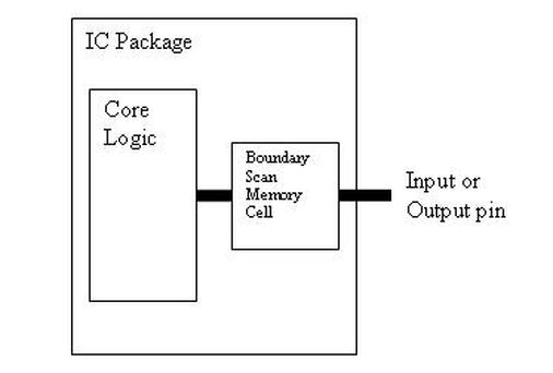 Figure 1. Boundary Scan memory cell between IC logic and external pin. Let’s take a more complete view of how this makes useful tests. 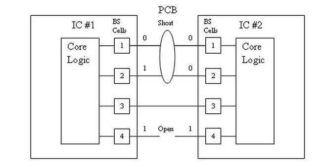 Figure 2. Shorts and Opens testing with boundary scan. Figure 2 shows how we can use boundary scan for testing for shorts and opens (the boundary scan cells are numbered for reference). The pins of the two ICs are connected together on the PCB. Keep in mind that these pins are routed to some other place on the PCB for a functional reason, the way the pins of IC 1 and 2 are connected is through the boundary scan cells, and these connections are just for testing. The whole boundary scan system is turned off when the board is actually being used and they have no affect. The short shown in Figure 2 is at the surface mount of the two pins on IC 1. Since we can read and write the contents of the boundary scan cells, we can set BS cell 1 on IC 1 to a 0 and BS cell on IC 1 to a 1 and read at IC 2 that both cells 1 and 2 read a 0. Similarly, since there is an open between the two 4 pins, the receiving pin will always show a 0. Boundary Scan Architecture There are four main parts to the boundary scan architecture. - Bypass Register - Instruction Register - Boundary Scan Register - Test Access Port (TAP) and TAP Controller The rest of these figures are from a really good boundary scan tutorial from Asset company (www.asset-intertech.com). There are four required pins that have to be added to an IC to operate the boundary scan system. - Test Data In (TDI) - Test Data Out (TDO) - Test Mode Select (TMS) - Test Clock (TCK) Figure 3 shows an IC with the boundary scan pins added to the package. 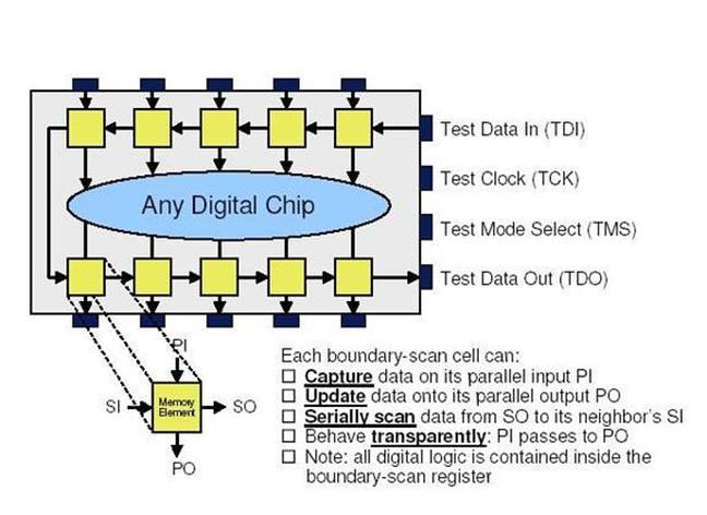 Figure 3. Boundary scan enabled IC. In Figure 3 you can see the parallel inputs and outputs along with the serial inputs and outputs. I talked about being able to read and write all of the individual boundary scan cells, this is accomplished with the serial input and output connections to each boundary scan memory cell. Data is written in and read out through TDI and TDO respectively in serial strings of zeros and ones. The TCK clock pin is used to clock this data in and out. TMS is a control signal used to coordinate all of these operations. Looking at Figure 4 we start to see how the four main pieces of boundary scan are setup. 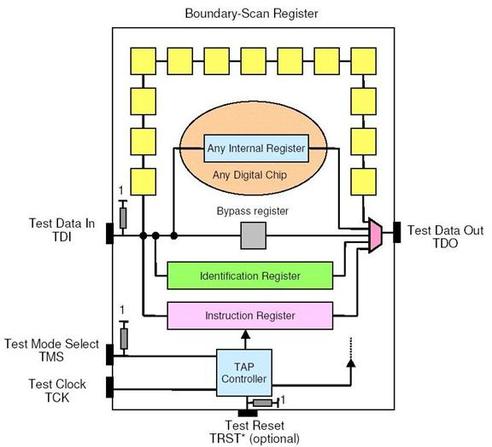 Figure 4. A boundary scan enabled IC showing boundary scan components In Figure 4 the yellow squares are the memory cells, these make up the boundary scan register. The Bypass register can be selected to put the IC into normal operation mode, bypassing the boundary scan system. The TAP controller is a state machine that interprets commands on the TMS input to control the boundary scan system. The instruction register controls the current operation of the boundary scan system and is programmed through the TDI input and controlled by the TAP controller. Although I didn’t mention it, Figure 4 shows an identification register. This can be used to store a unique identifier for that IC. Instruction Register The instruction register is where commands are loaded to the control the boundary scan system. Here are the steps to use the instruction register. 1. Using the TAP controller via the TMS input, the command is sent to connect the instruction register to TDI and TDO. This makes the register accessible to write commands to it. 2. A command in the form of a serial string is clocked into the instruction register using the TCK. 3. What are commands? The commands are putting the boundary scan system into useful configurations for testing. Here are some of the commands - Bypass – selects the bypass register between TDI and TDO - Sample – select the boundary scan register to TDI and TDO and sets the boundary scan cells to read the values being serially sent to them. - Preload – select the boundary scan register and sets the boundary scan cells to a known state. - Extest – select the boundary scan register and sets the boundary scan cells to a state where interconnect testing can be performed. Basically, isolates the IC logic for interconnect testing. - Intest - the boundary scan register and sets the boundary scan cells to apply their values to the internal IC logic. - Idcode – connects the identification register. - Clamp – This clamps the output pins to a constant state - Highz – puts the output pins in a highz state as in a tri-state output. 4. Upon sending the command to do so from the TAP controller, the command that was shifted into the instruction register is applied and takes effect on the system. Test Access Port and Controller When talking about the test access port that is really just the four inputs: TDI, TDO, TMS, TCK. The TAP Controller is where the TMS and TCK signal are interpreted. The TAP controller is implemented as a state machine that transitions states on the rising edge of TCK according to the value on TMS and updates the output from the TAP controller on the falling edge of TCK. Figure 5 shows the TAP controller state machine. 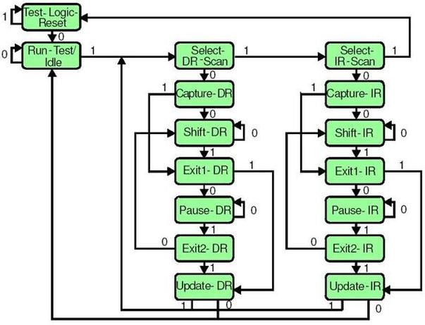 Figure 5. The TAP controller state machine. The arrows show the possible transitions and the numbers listed on the arrows are the TMS values that create that transition. There are states for the IR (instruction) register and the DR (boundary scan data) register. Going back to the procedure given in the instruction register section, sending a 0 – 1 – 1 would select the Instruction register. Then, holding TMS at 0 for the appropriate number of TCK high transitions would shift the command into the Instruction register. Finally, a 1 – 1 would update the Instruction register, update is what applies the command to the system. With the command sent, the states can continue on to the DR portion for shifting in test data strings. Boundary Scan Register The boundary scan cells located on the inputs and outputs pins are linked together in a serial string to form the boundary scan register. Figure 6 shows an example of how a boundary scan cell is designed. 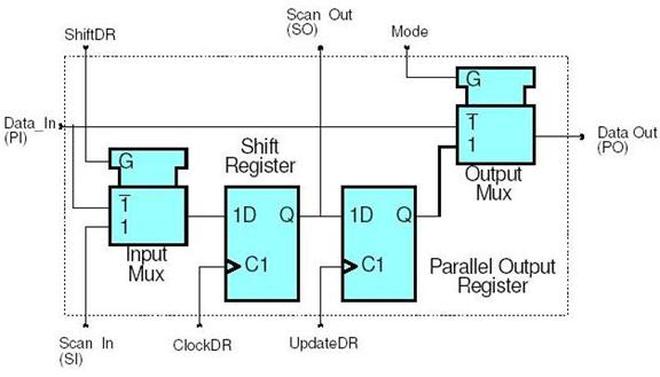 Figure 6. Boundary Scan Cell Design
Summary While there are endless topics that could be addressed related to boundary scan, I’ll leave it with the basics. The basic operation of boundary scan is - Scan in an instruction and apply it. - Scan in data and used it for testing. - Read back the data to find interconnect defects. The main pieces are - Instruction Register - Boundary Scan Data Register - Bypass Register - TAP and TAP Controller Comments are closed.
|
Archives
December 2022
Categories
All

|
 RSS Feed